Showing posts with label Gate. Show all posts

Tuesday, 3 November 2015

Gate 2016 - Apply Online, Aptitude Tests, Dates, Eligibility

Graduate Aptitude Test in Engineering (GATE 2016)

gate 2016

GATE is a Graduate Aptitude Test in Engineering conducted by IISc Banglore for admissions to M.TECH, M.E courses at IITs and NITs and many more private universities accross India. The GATE exam will be conducted from January 30 to February 07, 2016 (Saturdays and Sundays only)

The IISc Banglore and all the IITs organize this examination along with Human Resource Development, Department of Higher Education and the Government of India.
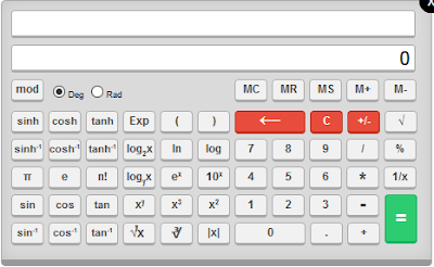

gate 2016 virtual calculator

GATE 2016 will be held for a total of 23 papers inclusive of a new one -Petroleum Engineering. There is provision for a buffer session on February 20, 2016 which may be used to hold the exam in case of any unforeseen circumstances.

You can download this pdf regarding Petroleum engineering syllabus

Here are the zones which will organize the examine:

Zone 1: Indian Institute of Science Bangalore - The Organizing Institute for GATE 2016

Zone 2: Indian Institute of Technology Bombay

Zone 3: Indian Institute of Technology Delhi

Zone 4: Indian Institute of Technology Guwahati

Zone 5: Indian Institute of Technology Kanpur

Zone 6: Indian Institute of Technology Kharagpur

Zone 7: Indian Institute of Technology Madras

Zone 8: Indian Institute of Technology Roorkee


Important Dates

GATE Online Application Processing System (GOAPS) Website Opens for Enrollment, Application Filling, Application Submission- September 1, 2015 (Tuesday)          

Last Date for Submission of Online Application through Website - October 8, 2015 (Thursday)       

Last Date for Request for Change in the Choice of Examination City via GOAPS login- November 20, 2015 (Friday)

Availability of Admit Card on the Online Application Interface for printing- December 17, 2015 (Thursday)

GATE 2016 Online Examination

  •     Forenoon: 9.00 AM to 12.00 Noon  January 30 to February 07, 2016
  •     Afternoon: 2.00 PM to 5.00 PM
  •     (On Saturdays and Sundays only)
Announcement of Results on the Online Application Website - March 19, 2016 (Saturday)
                               

You can check out Gate Syllabus Here

What's new this year?


  •     Online Calculator- Candidates will have to use the online virtual calculator that will be provided during the exam. Physical calculators will not be allowed.

  •     Revised Syllabus- The GATE Syllabi has been revised. Candidates must check the revised GATE 2016 Syllabus for their preparation

  •     New Paper- A new Paper has been introduced from GATE 2016  namely Petroleum Engineering

  •     Provision of GATE Answer Key: The GATE 2016 Answer Key will be provided after the exam is over for candidates to check. They can challenge the GATE 2016 Answer Key on payment of a nominal fee for a specified period of time.

GATE 2016 Exam Pattern: 


The GATE Paper comprises of two types of questions - Multiple Choice Questions and Numerical Questions. Multiple Choice Questions will have a correct answer from four options given while Numerical Questions have to be calculated and answered with the help of of a keypad. The GATE 2016 Question Paper will be designed to test students on their comprehension and application skills, recall as well as analytical abilities.

It may be noted that General Aptitude Questions are compulsory for all papers and will carry  questions for 15 marks.

GATE 2016 Exam Pattern as per the Paper code is as follows:


  •     Papers with codes AE, AG, BT, CE, CH, CS, EC, EE, IN, ME, MN, MT, PI, TF and XE: Engineering Mathematics (15% of total marks), General Aptitude section (15% of total marks) and  Main subject of the paper (70% percentage of the total marks).

  •     Papers with codes AR, CY, EY, GG, MA, PH and XL: General Aptitude section (15% of total marks) and  Main subject of the paper (85% percentage of the total marks).
Note:


  • GATE 2016  XE Paper will have a compulsory section in Engineering Mathematics and General Aptitude along with any two of XE sections B to G.
  • GATE 2016 XL Paper Pattern will have a compulsory section inSection H in Chemistry and General Aptitude along with any two of XL sections I to M


Eligible Qualifying Degree Eligibility of the Candidates as per the academic year of passing
B.E./B.Tech/ B.Arch/ B.Pharm. ( 4 years after 10+2) Currently in the 4th year or already completed
B.S (Post-Diploma/ 4 years after 10+2) Currently in the 4th year or already completed
M.Sc./M.A./ MCA or equivalent Currently in the final year or already completed
Int. M.E/ M.Tech (Post BSc) (Four year programme) Currently in the 2nd/3rd/4th year or already completed
Integrated M.E./M.Tech or 5 year Dual Degree (after Diploma or 10+2) - Currently in the 4th/5th year or already completed
Integrated M. Sc/ Integrated 5 year B.S.-M.S. Currently in the final year or already completed
Professional Society Examinations (equivalent to B.E/B.Tech/B.Arch)

Completed Section A or equivalent of such professional courses


Before going to exam do check Examinations Tips to keep your calm

Tuesday, 22 September 2015

GATE Electronic Devices Multiple Choice Questions With Answers

3.0 Electronics Devices


Gate 2016 Multiple Choice Questions (MCQ's)

MCQ 3.1
Drift current in the semiconductors depends upon
(A) only the electric field
(B) only the carrier concentration gradient
(C) both the electric field and the carrier concentration
(D) both the electric field and the carrier concentration gradient


 MCQ 3.2
A Zener diode, when used in voltage stabilization circuits, is biased in
(A) reverse bias region below the breakdown voltage
(B) reverse breakdown region
(C) forward bias region
(D) forward bias constant current mode


MCQ 3.3
A silicon PN junction is forward biased with a constant current at
room temperature. When the temperature is increased by 10ºC, the
forward bias voltage across the PN junction
(A) increases by 60 mV
(B) decreases by 60 mV
(C) increases by 25 mV
(D) decreases by 25 mV 


MCQ 3.6
At room temperature, a possible value for the mobility of electrons in
the inversion layer of a silicon n-channel MOSFET is
(A) 450 cm2/V-s 

(B) 1350 cm2/V-s
(C) 1800 cm2/V-s 

(D) 3600 cm2/V-s 

MCQ 3.7
Thin gate oxide in a CMOS process in preferably grown using
(A) wet oxidation 

(B) dry oxidation
(C) epitaxial oxidation 

(D) ion implantation 

MCQ 3.8
In a uniformly doped BJT, assume that NE,NB and NC are the
emitter, base and collector doping in atoms/cm3, respectively. If the
emitter injection efficiency of the BJT is close unity, which one of the
following condition is TRUE
(A) NE = NB = NC (B) NE >> NB and NB > NC
(C) NE = NB and NB < NC (D) NE < NB < NC


MCQ 3.9
Compared to a p-n junction with Na Nd 10^14 /cu.cm
which one of the following statements is TRUE for a p-n junction with
Na=Nd=10^20 /cu.cm

(A) Reverse breakdown voltage is lower and depletion capacitance is
lower
(B) Reverse breakdown voltage is higher and depletion capacitance is
lower
(C) Reverse breakdown voltage is lower and depletion capacitance is
higher
(D) Reverse breakdown voltage is higher and depletion capacitance is
higher


Statements for Linked Answer Question : 3.10 & 3.11 :
The silicon sample with unit cross-sectional area shown below is in
thermal equilibrium. The following information is given: T = 300 K
electronic charge 1.6 x 10^19 C = # − , thermal voltage = 26 mV and
electron mobility = 1350 cm.sq/V-s 


MCQ 3.10
The magnitude of the electric field at x = 0.5 μm is
(A) 1 kV/cm 

(B) 5 kV/cm
(C) 10 kV/cm 

(D) 26 kV/cm 

MCQ 3.11
The magnitude of the electron of the electron drift current density at
x = 0.5 μm is
(A) 2.16 10^4 A/cm^2 

(B) 1.08 10^4 A/m^2
(C) 4.32 10^3 A/cm^2

(D) 6.48 10^2 A/cm^2 

MCQ 3.12
In an n-type silicon crystal at room temperature, which of the
following can have a concentration of 4 x 10^19 # cm^-3?
(A) Silicon atoms 

(B) Holes
(C) Dopant atoms 

(D) Valence electrons 

MCQ 3.13
The ratio of the mobility to the diffusion coefficient in a semiconductor
has the units
(A) V^-1 (B) cm.V^1
(C) V.cm-1 (D) V.s

  
MCQ 3.14
Consider the following two statements about the internal conditions
in a n −channel MOSFET operating in the active region.
S1 : The inversion charge decreases from source to drain
S2 : The channel potential increases from source to drain.
Which of the following is correct?
(A) Only S2 is true
(B) Both S1 and S2 are false
(C) Both S1 and S2 are true, but S2 is not a reason for S1
(D) Both S1 and S2 are true, and S2 is a reason for S1


Common Date for Question 3.13 and 3.14
Consider a silicon p − n junction at room temperature having the
following parameters:
Doping on the n-side 1 x 10^17cm-3
Depletion width on the n-side =  0.1μm
Depletion width on the p −side = 1.0μm
Intrinsic carrier concentration = 1.4 x 10^10 cm-3
Thermal voltage = 26 mV
Permittivity of free space = 8.85 x 10^14 - F.cm-1
Dielectric constant of silicon = 12


 MCQ 3.15
The built-in potential of the junction
(A) is 0.70 V
(B) is 0.76 V
(C) is 0.82 V
(D) Cannot be estimated from the data given


MCQ 3.16
The peak electric field in the device is
(A) 0.15 MV . cm-1, directed from p −region to n −region

(B) 0.15 MV . cm-1, directed from n −region to p −region
(C) 1.80 MV . cm-1, directed from p-retion to n −region
(D) 1.80 MV . cm-1, directed from n −region to p −region


MCQ 3.17
Which of the following is NOT associated with a p − n junction ?
(A) Junction Capacitance (B) Charge Storage Capacitance
(C) Depletion Capacitance (D) Channel Length Modulations


MCQ 3.18
Which of the following is true?
(A) A silicon wafer heavily doped with boron is a p+ substrate
(B) A silicon wafer lightly doped with boron is a p+ substrate
(C) A silicon wafer heavily doped with arsenic is a p+ substrate
(D) A silicon wafer lightly doped with arsenic is a p+ substrate


MCQ 3.19
A silicon wafer has 100 nm of oxide on it and is furnace at a temperature
above 1000 Degree Celsius for further oxidation in dry oxygen. The oxidation rate
(A) is independent of current oxide thickness and temperature
(B) is independent of current oxide thickness but depends on
temperature
(C) slows down as the oxide grows
(D) is zero as the existing oxide prevents further oxidation


MCQ 3.22
Silicon is doped with boron to a concentration of 4 x 10^17 # atoms cm3
Assume the intrinsic carrier concentration of silicon to be 1.5 x 10^10/cm3 

and the value of kT/q to be 25 mV at 300 K. Compared to
undopped silicon, the fermi level of doped silicon
(A) goes down by 0.31 eV (B) goes up by 0.13 eV
(C) goes down by 0.427 eV (D) goes up by 0.427 eV


MCQ 3.23
The cross section of a JFET is shown in the following figure. Let
Vc be −2 V and let Vp

be the initial pinch -off voltage. If the width
W is doubled (with other geometrical parameters and doping levels
remaining the same), then the ratio between the mutual trans
conductances of the initial and the modified JFET is


MCQ 3.24
Consider the following assertions.
S1 : For Zener effect to occur, a very abrupt junction is required.
S2 : For quantum tunneling to occur, a very narrow energy barrier is
required.
Which of the following is correct ?
(A) Only S2 is true
(B) S1 and S2 are both true but S2 is not a reason for S1
(C) S1 and S2 and are both true but S2 is not a reason for S1
(D) Both S1 and S2 are false


MCQ 3.26
In a p+n junction diode under reverse biased the magnitude of electric field is maximum at
(A) the edge of the depletion region on the p-side
(B) the edge of the depletion region on the n-side
(C) the p+n junction
(D) the centre of the depletion region on the n-side


MCQ 3.27
Group I lists four types of p − n junction diodes. Match each device
in Group I with one of the option in Group II to indicate the bias
condition of the device in its normal mode of operation.
Group - I Group-II
(P) Zener Diode                        (1) Forward bias
(Q) Solar cell                            (2) Reverse bias
(R) LASER diode
(S) Avalanche Photodiode


(A) P - 1, Q - 2, R - 1, S - 2
(B) P - 2, Q - 1, R - 1, S - 2
(C) P - 2, Q - 2, R - 1, S- -2
(D) P - 2, Q - 1, R - 2, S - 2


MCQ 3.28
Group I lists four different semiconductor devices. match each device
in Group I with its charactecteristic property in Group II

Group-I                                                  Group-II
(P) BJT                                         (1) Population iniversion
(Q) MOS capacitor                         (2) Pinch-off voltage
(R) LASER diode                            (3) Early effect
(S) JFET                                       (4) Flat-band voltage


(A) P - 3, Q - 1, R - 4, S - 2
(B) P - 1, Q - 4, R - 3, S - 2
(C) P - 3, Q - 4, R - 1, S - 2
(D) P - 3, Q - 2, R - 1, S - 4


MCQ 3.29
A p+n junction has a built-in potential of 0.8 V. The depletion layer
width a reverse bias of 1.2 V is 2 μm. For a reverse bias of 7.2 V, the
depletion layer width will be
(A) 4 μm (B) 4.9 μm
(C) 8 μm (D) 12 μm


MCQ 3.30
The DC current gain (β) of a BJT is 50. Assuming that the emitter
injection efficiency is 0.995, the base transport factor is
(A) 0.980 (B) 0.985
(C) 0.990 (D) 0.995


Common Data Question 2.29, 2.30 and 2.31 : 


MCQ 3.31
The gate oxide thickness in the MOS capacitor is
(A) 50 nm (B) 143 nm
(C) 350 nm (D) 1 μm


MCQ 3.32
The maximum depletion layer width in silicon is
(A) 0.143 μm (B) 0.857 μm
(C) 1 μm (D) 1.143 μm


MCQ 3.33
Consider the following statements about the C − V characteristics
plot :
S1 : The MOS capacitor has as n-type substrate
S2 : If positive charges are introduced in the oxide, the C − V polt
will shift to the left.
Then which of the following is true?
(A) Both S1 and S2 are true
(B) S1 is true and S2 is false
(C) S1 is false and S2 is true
(D) Both S1 and S2 are false


MCQ 3.34
The values of voltage (VD) across a tunnel-diode corresponding to
peak and valley currents are Vp,VD respectively. The range of tunneldiode
voltage for VD which the slope of its I − VD characteristics is negative would be
(A) VD < 0 (B) 0 <= VD < Vp
(C) Vp <= VD < Vv (D) VD >= Vv


MCQ 3.35
The concentration of minority carriers in an extrinsic semiconductor
under equilibrium is
(A) Directly proportional to doping concentration
(B) Inversely proportional to the doping concentration
(C) Directly proportional to the intrinsic concentration
(D) Inversely proportional to the intrinsic concentration


MCQ 3.36
Under low level injection assumption, the injected minority carrier
current for an extrinsic semiconductor is essentially the
(A) Diffusion current (B) Drift current
(C) Recombination current (D) Induced current


MCQ 3.37
The phenomenon known as “Early Effect” in a bipolar transistor
refers to a reduction of the effective base-width caused by
(A) Electron - hole recombination at the base
(B) The reverse biasing of the base - collector junction
(C) The forward biasing of emitter-base junction
(D) The early removal of stored base charge during saturation-to-cut
off switching


MCQ 3.38
In the circuit shown below, the switch was connected to position 1 at
t < 0 and at t = 0, it is changed to position 2. Assume that the diode
has zero voltage drop and a storage time ts . For 0 < t # ts, vR is given
by (all in Volts)


MCQ 3.39
The majority carriers in an n-type semiconductor have an average
drift velocity v in a direction perpendicular to a uniform magnetic
field B. The electric field E induced due to Hall effect acts in the
direction
(A) v x B (B) B x v
(C) along v (D) opposite to v


MCQ 3.40
Find the correct match between Group 1 and Group 2
Group 1 Group 2
E - Varactor diode                  1. Voltage reference
F - PIN diode                          2. High frequency switch
G - Zener diode                     3. Tuned circuits
H - Schottky diode                 4. Current controlled attenuator


(A) E - 4, F - 2, G - 1, H - 3
(B) E - 3, F - 4, G - 1, H - 3
(C) E - 2, F - 4, G - 1, H - 2
(D) E - 1, F - 3, G - 2, H - 4


MCQ 3.41
A heavily doped n- type semiconductor has the following data:
Hole-electron ratio :0.4
Doping concentration :4.2 x 10^8 atoms/m
^3
Intrinsic concentration :1.5 x 10
^4 atoms/m^3

The ratio of conductance of the n −type semiconductor to that of the
intrinsic semiconductor of same material and ate same temperature
is given by
(A) 0.00005 (B) 2000
(C) 10000 (D) 20000


MCQ 3.42
The bandgap of Silicon at room temperature is
(A) 1.3 eV (B) 0.7 eV
(C) 1.1 eV (D) 1.4 eV
 

MCQ 3.43
A Silicon PN junction at a temperature of 20c C has a reverse
saturation current of 10 pico - Ameres (pA). The reserve saturation
current at 40
°C for the same bias is approximately
(A) 30 pA (B) 40 pA
(C) 50 pA (D) 60 pA


MCQ 3.44
The primary reason for the widespread use of Silicon in semiconductor
device technology is
(A) abundance of Silicon on the surface of the Earth.
(B) larger bandgap of Silicon in comparison to Germanium.
(C) favorable properties of Silicon - dioxide (SiO2)
(D) lower melting point


MCQ 3.45
A Silicon sample A is doped with 10^18 atoms/cm
^3 of boron. Another
sample B of identical dimension is doped with 10
^18 atoms/cm^3
phosphorus. The ratio of electron to hole mobility is 3. The ratio of
conductivity of the sample A to B is


(A) 3     (B)1/3
(C)2/3   (D)3/2


MCQ 3.46
Consider the following statements S1 and S2.
S1 : The threshold voltage (VT) of MOS capacitor decreases with
increase in gate oxide thickness.
S2 : The threshold voltage (VT) of a MOS capacitor decreases with
increase in substrate doping concentration.
 

Which Marks of the following is correct ?
(A) S1 is FALSE and S2 is TRUE
(B) Both S1 and S2 are TRUE
(C) Both S1 and S2 are FALSE
(D) S1 is TRUE and S2 is FALSE


MCQ 3.47The longest wavelength that can be absorbed by silicon, which has
the bandgap of 1.12 eV, is 1.1 μm. If the longest wavelength that can
be absorbed by another material is 0.87 μm, then bandgap of this
material is
(A) 1.416 A/cm2 (B) 0.886 eV
(C) 0.854 eV (D) 0.706 eV


MCQ 3.48
n-type silicon is obtained by doping silicon with
(A) Germanium (B) Aluminium
(C) Boron (D) Phosphorus


MCQ 3.49
The Bandgap of silicon at 300 K is
(A) 1.36 eV (B) 1.10 eV
(C) 0.80 eV (D) 0.67 eV


MCQ 3.50
Choose proper substitutes for X and Y to make the following
statement correct Tunnel diode and Avalanche photo diode are
operated in X bias ad Y bias respectively
(A) X: reverse, Y: reverse (B) X: reverse, Y: forward
(C) X: forward, Y: reverse (D) X: forward, Y: forward


Comment below for answers

10 Unexpected Interview Questions and Answers
Entc Engg. Powered by Blogger.